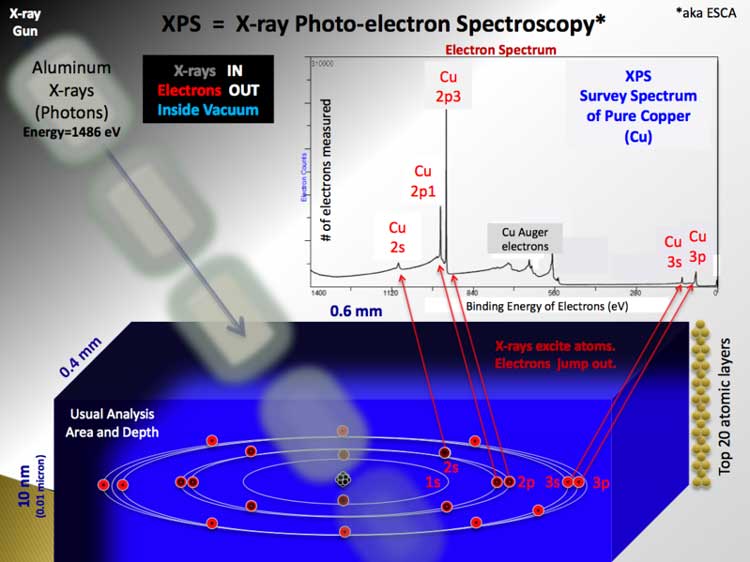
X-ray photoelectron spectroscopy (XPS) is a quantitative spectroscopic technique that measures the elemental composition, empirical formula, chemical state and electronic state of the elements that exist within a material. XPS spectra are obtained by irradiating a material with a beam of X-rays while simultaneously measuring the kinetic energy and number of electrons that escape from the top 1 to 10 nm of the material being analyzed. XPS requires ultra high vacuum (UHV) conditions. XPS is a surface chemical analysis technique that can be used to analyze the surface chemistry of a material in its "as received" state, or after some treatment, for example: fracturing, cutting or scraping in air or UHV to expose the bulk chemistry, ion beam etching to clean off some of the surface contamination, exposure to heat to study the changes due to heating, exposure to reactive gases or solutions, exposure to ion beam implant, exposure to ultraviolet light. * XPS is also known as ESCA, an abbreviation for Electron Spectroscopy for Chemical Analysis.
Basic components of a monochromatic XPS system.
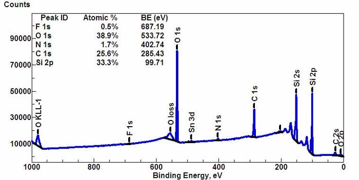
Wide-scan survey spectrum for all elements. (*)
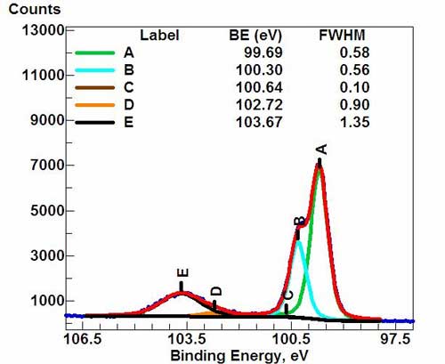
High-resolution spectrum for Si(2p) signal. (*)
Rough schematic of XPS physics - "Photoelectric Effect. XPS is used to measure: * elemental composition of the surface (top 1– 10 nm usually) XPS can be performed using either a commercially built XPS system, a privately built XPS system or a synchrotron-based light source combined with a custom designed electron analyzer. Commercial XPS instruments in the year 2005 used either a highly focused 20 to 200 micrometer beam of monochromatic aluminium Kα X-rays or a broad 10–30 mm beam of non-monochromatic (polychromatic) magnesium X-rays. A few, special design, XPS instruments can analyze volatile liquids or gases, materials at low or high temperatures or materials at roughly 1 torr vacuum, but there are relatively few of these types of XPS systems. Because the energy of a particular X-ray wavelength is known, the electron binding energy of each of the emitted electrons can be determined by using an equation that is based on the work of Ernest Rutherford (1914):
where Ebinding is the binding energy (BE) of the electron, Ephoton is the energy of the X-ray photons being used, Ekinetic is the kinetic energy of the electron as measured by the instrument and φ is the work function of the spectrometer (not the material). In 1887, Heinrich Rudolf Hertz discovered the photoelectric effect that was explained in 1905 by Albert Einstein (Nobel Prize in Physics 1921). Two years later, in 1907, P.D. Innes experimented with a Röntgen tube, Helmholtz coils, a magnetic field hemisphere (electron energy analyzer) and photographic plates to record broad bands of emitted electrons as a function of velocity, in effect recording the first XPS spectrum. Other researchers, Henry Moseley, Rawlinson and Robinson, independently performed various experiments trying to sort out the details in the broad bands. Wars halted research on XPS. After WWII, Kai Siegbahn and his group in Uppsala (Sweden) developed several significant improvements in the equipment and in 1954 recorded the first high energy resolution XPS spectrum of cleaved sodium chloride (NaCl) revealing the potential of XPS. A few years later in 1967, Siegbahn published a comprehensive study on XPS bringing instant recognition of the utility of XPS. In cooperation with Siegbahn, Hewlett-Packard in the USA produced the first commercial monochromatic XPS instrument in 1969. Siegbahn received the Nobel Prize in 1981 to acknowledge his extensive efforts to develop XPS into a useful analytical tool.[1] In parallel with Siegbahn's work, David Turner at Imperial College (and later at Oxford) in the UK developed ultraviolet photoelectron spectroscopy (UPS) on molecular species using helium lamps.[2] Physics A typical XPS spectrum is a plot of the number of electrons detected (sometimes per unit time) (Y-axis, ordinate) versus the binding energy of the electrons detected (X-axis, abscissa). Each element produces a characteristic set of XPS peaks at characteristic binding energy values that directly identify each element that exist in or on the surface of the material being analyzed. These characteristic peaks correspond to the electron configuration of the electrons within the atoms, e.g., 1s, 2s, 2p, 3s, etc. The number of detected electrons in each of the characteristic peaks is directly related to the amount of element within the area (volume) irradiated. To generate atomic percentage values, each raw XPS signal must be corrected by dividing its signal intensity (number of electrons detected) by a "relative sensitivity factor" (RSF) and normalized over all of the elements detected. To count the number of electrons at each kinetic energy value, with the minimum of error, XPS must be performed under ultra-high vacuum (UHV) conditions because electron counting detectors in XPS instruments are typically one meter away from the material irradiated with X-rays. It is important to note that XPS detects only those electrons that have actually escaped into the vacuum of the instrument. The photo-emitted electrons that have escaped into the vacuum of the instrument are those that originated from within the top 10 to 12 nm of the material. All of the deeper photo-emitted electrons, which were generated as the X-rays penetrated 1– 5 micrometers of the material, are either recaptured or trapped in various excited states within the material. For most applications, it is, in effect, a non-destructive technique that measures the surface chemistry of any material. Components of an XPS system The main components of a commercially made XPS system include: * A source of X-rays Monochromatic aluminium K-alpha X-rays are normally produced by diffracting and focusing a beam of non-monochromatic X-rays off of a thin disc of natural, crystalline quartz with a <1010> orientation. The resulting wavelength is 8.3386 angstroms (0.83386 nm) which corresponds to a photon energy of 1486.7 eV. The energy width of the monochromated X-rays is 0.16 eV, but the common electron energy analyzer (spectrometer) produces an ultimate energy resolution on the order of 0.25 eV which, in effect, is the ultimate energy resolution of most commercial systems. When working under practical, everyday conditions, high energy resolution settings will produce peak widths (FWHM) between 0.4–0.6 eV for various pure elements and some compounds. Non-monochromatic magnesium X-rays have a wavelength of 9.89 angstroms (0.989 nm) which corresponds to a photon energy of 1253 eV. The energy width of the non-monochromated X-ray is roughly 0.70 eV, which, in effect is the ultimate energy resolution of a system using non-monochromatic X-rays. Non-monochromatic X-ray sources do not use any crystals to diffract the X-rays which allows all primary X-rays lines and the full range of high energy Bremsstrahlung X-rays (1–12 keV) to reach the surface. The typical ultimate high energy resolution (FWHM) when using this source is 0.9–1.0 eV, which includes with the spectrometer-induced broadening, pass-energy settings and the peak-width of the non-monochromatic magnesium X-ray source. Uses and capabilities XPS is routinely used to determine: * What elements and the quantity of those elements that are present within the top 1-12 nm of the sample surface
* Measure uniformity of elemental composition across the top the surface (or line profiling or mapping)
The ability to produce Chemical State information from the topmost 1-12 nm of any surface makes XPS a unique and invaluable tool for understanding the chemistry of any surface either, as received, or after physical or chemical treatment(s). Because modern systems use monochromatic X-ray sources, XPS measurements leave the surface free of any degradation with few exceptions. Chemical state analysis of the surface of polymers readily reveals the presence or absence of the chemical states of carbon known as: carbide (C 2-), hydrocarbon (C-C), alcohol (C-OH), ketone (C=O), organic ester (COOR), carbonate (CO3), fluoro-hydrocarbon (CF2-CH2), trifluorocarbon (CF3). Chemical state analysis of the surface of a silicon wafer readily reveals the presence or absence of the chemical states of silicon known as: n-doped silicon, p-doped silicon, silicon suboxide (Si2O), silicon monoxide (SiO), Si2O3, silicon dioxide (SiO2). Industries that use XPS * Adhesion
Quantitative accuracy * XPS is widely used to generate empirical formula because it readily yields excellent quantitative accuracy from homogeneous solid state materials
* 1–10 minutes for a survey scan that measures the amount of all elements, 1– 10 minutes for high energy resolution scans that reveal chemical state differences, 1– 4 hours for a depth profile that measures 4– 5 elements as a function of etched depth (usual final depth is 1,000 nm)
* 0.1–1.0 at% (0.1 at% = 1 part per thousand = 1000 ppm). (Ultimate detection limit for most elements is approximately 100 ppm, which requires 8–16 hours.)
* Measured area depends on instrument design. The minimum analysis area ranges from 10 to 200 micrometres. Largest size for a monochromatic beam of X-rays is 1–5 mm. Non-monochromatic beams are 10–50 mm in diameter. Spectroscopic image resolution levels of 200 nm or below has been achieved on latest imaging XPS instruments using synchrotron radiation as X-ray source.
* Older instruments accept samples: 1×1 to 3×3 cm. Present systems can accept samples up to 30×30 cm.[citation needed]
* Depends on the sensitivity of the material to the wavelength of X-rays used, the total dose of the X-rays, the temperature of the surface and the level of the vacuum. Metals, alloys, ceramics and most glasses are not measurably degraded by either non-monochromatic or monochromatic X-rays. Some, but not all, polymers, catalysts, certain highly oxygenated compounds, various inorganic compounds and fine organics are degraded by either monochromatic or non-monochromatic X-ray sources.
Inorganic compounds, metal alloys, semiconductors, polymers, pure elements, catalysts, glasses, ceramics, paints, papers, inks, woods, plant parts, make-up, teeth, bones, human implants, biomaterials, viscous oils, glues, ion modified materials Organic chemicals are not routinely analyzed by XPS because they are readily degraded by either the energy of the X-rays or the heat from non-monochromatic X-ray sources. Analysis details * Low-voltage electron beam (1-20 eV) (or electron flood gun)
* Sample handling
Peak identification The identification of peaks in any survey spectrum is possible because Prof. Kai Siegbahn improved the energy resolution of his XPS instrument to the point that observed signals were both tall and narrow with respect to the energy range measured (0-1400 eV). In the course of improving his XPS instruments, he collected spectra from pure conductive elements. That collection of spectra yielded peaks with energies (reported as BEs) that are characteristic for each specific element. The number of peaks produced by a single element varies from 1 to more than 20. Tables of binding energies (BEs) that identify the shell and spin-orbit of each peak produced by a given element are included with modern XPS instruments, and can be found in various handbooks and websites . Because these experimentally determined BEs are characteristic of specific elements, they can be directly used to identify experimentally measured peaks of a material with unknown elemental composition. Before beginning the process of peak identification, the analyst must determine if the BEs of the unprocessed survey spectrum (0-1400 eV) have or have not been shifted due to a positive or negative surface charge. This is most often done by looking for two peaks that due to the presence of carbon and oxygen. {tbc} Charge referencing insulators Charge referencing is needed when a sample suffers either a positive (+) or negative (-) charge induced shift of experimental BEs. Charge referencing is needed to obtain meaningful BEs from both wide-scan, high sensitivity (low energy resolution) survey spectra (0-1100 eV), and also narrow-scan, chemical state (high energy resolution) spectra. Charge induced shifting causes experimentally measured BEs of XPS peaks to appear at BEs that are greater or smaller than true BEs. Charge referencing is performed by adding or subtracting a "Charge Correction Factor" to each of the experimentally measured BEs. In general, the BE of the hydrocarbon peak of the C (1s) XPS signal is used to charge reference (charge correct) all BEs obtained from non-conductive (insulating) samples or conductors that have been deliberately insulated from the sample mount. Charge induced shifting is normally due to: a modest excess of low voltage (-1 to -20 eV) electrons attached to the surface, or a modest shortage of electrons (+1 to +15 eV) within the top 1-12 nm of the sample caused by the loss of photo-emitted electrons. The degree of charging depends on various factors. If, by chance, the charging of the surface is excessively positive, then the spectrum might appear as a series of rolling hills, not sharp peaks as shown in the example spectrum. The C (1s) BE of the hydrocarbon species (moieties) of the "Adventitious" carbon that appears on all, air-exposed, conductive and semi-conductive materials is normally found between 284.5 eV and 285.5 eV. For convenience, the C (1s) of hydrocarbon moieties is defined to appear between 284.6 eV and 285.0 eV. A value of 284.8 eV has become popular in recent years. However, some recent reports indicate that 284.9 eV or 285.0 eV represents hydrocarbons attached on metals, not the natural native oxide.[citation needed] The 284.8 eV BE is routinely used as the "Reference BE" for charge referencing insulators. When the C (1s) BE is used for charge referencing, then the charge correction factor is the difference between 284.8 eV and the experimentally measured C (1s) BE of the hydrocarbon moieties. When using a monochromatic XPS system together with a low voltage electron flood gun for charge compensation the experimental BEs of the C (1s) hydrocarbon peak is often 4-5 eV smaller than the reference BE value (284.8 eV). In this case, all experimental BEs appear at lower BEs than expected and need to be increased by adding a value ranging from 4 to 5 eV. Non-monochromatic XPS systems are not usually equipped with a low voltage electron flood gun so the BEs will normally appear at higher BEs than expected. It is normal to subtract a charge correction factor from all BEs produced by a non-monochromatic XPS system. Conductive materials and most native oxides of conductors should never need charge referencing. Conductive materials should never be charge referenced unless the topmost layer of the sample has a thick non-conductive film. Peak-fitting The process of peak-fitting high energy resolution XPS spectra is still a mixture of art, science, knowledge and experience. The peak-fit process is affected by instrument design, instrument components, experimental settings (aka analysis conditions) and sample variables. Most instrument parameters are constant while others depend on the choice of experimental settings. Before starting any peak-fit effort, the analyst performing the peak-fit needs to know if the topmost 15 nm of the sample is expected to be a homogeneous material or is expected to be a mixture of materials. If the top 15 nm is a homogeneous material with only very minor amounts of adventitious carbon and adsorbed gases, then the analyst can use theoretical peak area ratios to enhance the peak-fitting process. Variables that affect or define peak-fit results include: * FWHMs
When using high energy resolution experiment settings on an XPS equipped with a monochromatic Al K-alpha X-ray source, the FWHM of the major XPS peaks range from 0.3 eV to 1.7 eV. The following is a simple summary of FWHM from major XPS signals: * Main metal peaks (e.g. 1s, 2p3, 3d5, 4f7) from pure metals have FWHMs that range from 0.30 eV to 1.0 eV
Chemical shift values depend on the degree of electron bond polarization between nearest neighbor atoms. A specific chemical shift is the difference in BE values of one specific chemical state versus the BE of the pure element. (refer to chemical state listed in Wikipedia) Peaks derived from peak-fitting a raw chemical state spectrum are due to the presence of different chemical states. Peakshapes Depends on instrument parameters, experimental parameters and sample characteristics
FWHM and purity of X-rays used (monochromatic Al, non-monochromatic Mg, Synchrotron, Ag, Zr...)
Settings of the electron analyzer (e.g. pass energy, step size)
Physical form of the sample (single crystal, polished, powder, corroded...)
Related methods * UPS, Ultra-violet photoelectron spectroscopy
* Annotated Handbooks of Monochromatic XPS Spectra, PDF of Volumes 1 and 2, B.V.Crist, published by XPS International LLC, 2005, Mountain View, CA, USA
* Online lecture- Introduction to X-ray Photoelectron Spectroscopy and to XPS Applications by Dmitry Zemlyanov
* Photoemission spectroscopy
X-ray photoelectron spectroscopy of solid surfaces, Vadim Ivanovich Nefedov References 1. ^ Electron Spectroscopy for Atoms, Molecules and Condensed Matter, Nobel Lecture, December 8, 1981 Retrieved from "http://en.wikipedia.org/" |
|


